 五度妙笔
五度妙笔 API商城
API商城
 数据库
数据库Untrusted Analog Components Add Risks For Critical Infrastructure
Key Takeaways
- New certificate-based solutions are necessary within fabs and packaging houses to deliver trusted semiconductors.
- Physical IDs bind the device to the certificate, but it needs to be immutable and unclonable.
- Extrinsic IDs are required for analog, mixed-signal, sensor ICs as well as discrete components.
Rising concern over the source and destination of chips, and the components within them, is driving a global effort to tag them in a way that is permanent, immutable, and unclonable.
While these types of efforts are gaining traction in the digital world, analog/mixed signal content in chips and systems lacks such tags. The absence of ID technology leaves them vulnerable to counterfeits and thus compromises the end system’s performance. This exposure to counterfeits also includes sensors and discrete components. All of these components are used in critical infrastructure and security-sensitive markets, as well as in complex systems that are subject to import/export restrictions. The challenge now is to remove these exposures by using end-to-end tracking of physical IDs that support a trusted supply chain solution. But it’s not so simple.
A physical ID is a linchpin technology. It can be read during manufacturing and in the field, but it needs to be immutable and unclonable. However, while digital ICs can leverage available ID technology, there is no equivalent for mixed-signal/analog ICs, sensor ICs, or discrete components. This is a problem for critical infrastructure (as defined by the U.S. government) in the telecommunication, aerospace, defense, and utility sectors, which comprise roughly 20% of today’s global semiconductor total addressable market (TAM), or about $150 billion.
A trusted supply chain provides a secure digital layer of certificates that are shared across the electronics ecosystem — wafer, packaged unit, PCB, and end system.
“At the core of a trusted supply chain lies a physical trust anchor, an immutable device identity that is inseparably linked to its digital certificate,” said Daniel DiMase, CEO of Aerocyonics. “This anchor can take several forms, depending on device class and manufacturing process, such as a physically unclonable function (PUF) derived from intrinsic silicon variation; a secure element or cryptographic dielet embedded during wafer fabrication; a laser-etched or fused die ID tied to a certificate in the fab’s database; or a non-volatile memory signature coupled with a one-time programmable key vault. Each provides a hardware-rooted identity that cannot be cloned or altered without detection. This anchor, embedded at the wafer or die stage, establishes a verifiable and unclonable bond between the physical silicon and its certified digital record.”
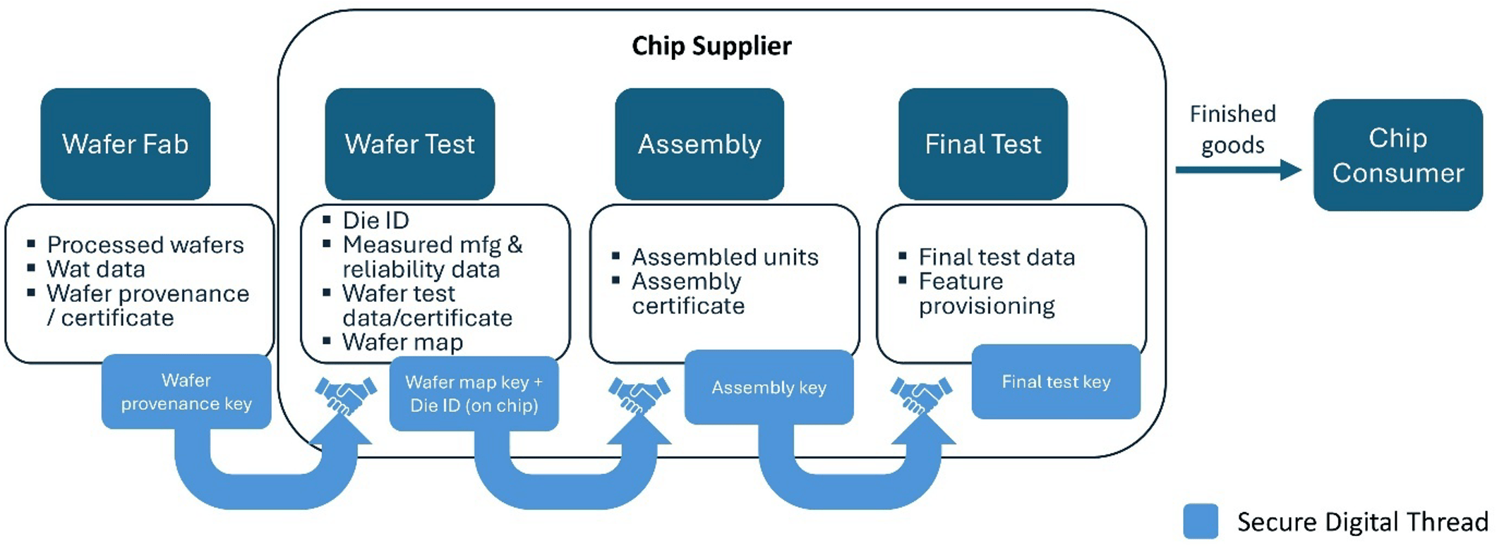
Fig. 1: Certification generation along the manufacturing ecosystem. Source: Tartan Silicon Systems
Device ID technology works in concert with wafer and packaged-unit manufacturing test processes.
“There are two main scenarios to consider when creating a device-level ID and certificate,” said Alan Arnoff, president and CEO at Tartan Silicon Systems. “The first is assigning a unique device ID, and the second is provisioning the device with specific features or keys. That provision typically happens at final test once the device’s functionality has been fully verified. In terms of the unique device ID, there are a couple of ways to generate and link it to a certificate. One approach is a zero-touch method, where the ID is created automatically at power-up using an on-chip digital fingerprint. This is typically implemented with a PUF or a root-of-trust (RoT) block. Another approach is to establish the ID during wafer test. In this case, the ID is read and recorded alongside wafer test data, which allows you to tie it back to the wafer ID and the die’s exact location. That information becomes part of the overall traceability database.”
Identifier technologies
Physical IDs for devices are foundational technology for a trusted supply chain solution. Physical IDs need to be unique. Historically, manufacturers have used simple optical IDs and electronic chip IDs (ECIDs) to provide device traceability. But unless they are immutable and unclonable, they still can be duplicated or tampered with.
A physical ID is something that can be ‘read.’ Intrinsic die IDs require the die/device to be powered on, which enables the ID to be electrically ‘set’ and ‘read.’ Extrinsic IDs can be read using optical, X-ray, or IR detectors, depending upon the technology.
Intrinsic
Digital VLSI products historically have relied upon an ECID to provide a unique identifier and support unit-level traceability (ULT) applications. Typically, an ECID contains wafer lot and wafer ID, the x,y wafer location, and test program version. Non-volatile memory bits are programmed during wafer test and additional ones during package-level test. Yet ECIDs are no longer adequate for either chip security nor trusted supply chain solutions.
“There is an increasing demand on the factories to provide provenance. In terms of what they’re doing today, we see a number of different things happening. At a minimum level, they are hard-coding unique identification into the silicon. That’s okay, but from a security perspective, it’s not the best approach. Having some form of on-die means to create a unique identification for each silicon die is becoming more desirable,” said Lee Harrison, director of Tessent IC solutions at Siemens EDA.
The shift to intrinsic IDs that meet security standards has been happening for the last decade. These IDs overwhelmingly rely upon the entropy in CMOS devices. These approaches create unique, immutable and unclonable identifiers. The table below lists approaches that represent state of the art.
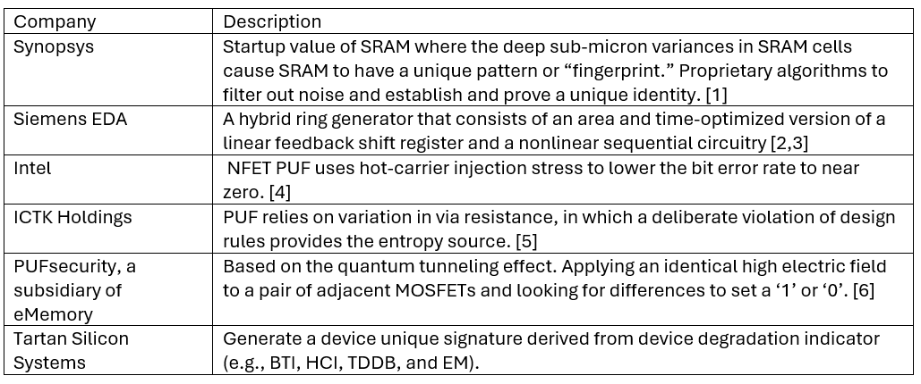
Table 1: Immutable intrinsic identifiers, by vendor.
Today, most of the intrinsic IDs are too costly for many edge/IoT devices. They consume silicon area and power, they require extra time to implement, and they may even complicate their own testability. But work is underway to change that.
“There are low footprint alternatives available,” said Reed Hinkel, director of strategic programs at Synopsys. “We can enable a very small footprint version that addresses these use cases, and it can be accessed through the lifecycle on test or debug interfaces. As far as process nodes, our IP has been used successfully on every CMOS process node, beginning at 350nm and targeted for nodes at 2nm — and soon, angstrom nodes. As long as SRAM exists in a process node, our IP works.”
In recently published papers, Siemens engineers described a low-cost solution [4,5]. “This work presents a simple, yet effective, all-digital, lightweight, and self-testable random number generator to produce a nonce. It builds on a generic ring generator architecture, i.e., an area- and time-optimized version of a linear feedback shift register, driven by a multiple-output ring oscillator. A comprehensive evaluation, based on three statistical test suites from the National Institute of Standards and Technology and BSI, shows feasibility and efficiency of the proposed scheme…”[4].
Extrinsic
There are multiple use cases for extrinsic IDs. They can be read even when the device is not powered on. They facilitate tracing components in assembly and PCB factories. Semiconductor manufacturers have long used laser-scribed IDs on wafers and 2D dot matrices for substrates and package lids. However, these approaches do not meet the ID requirements of a trusted supply chain. Intrinsic IDs also do not support most analog/mixed-signal, MEMS, sensor ICs, or discrete components such as power transistors and capacitors.
“Many approaches such as those based on encrypted keys require the device to be powered up, and this is true for a large portion of existing solutions,” said Melissa Grupen-Shemansky, CTO at SEMI. “Some approaches are exploring the use of externally applied or embedded physically unclonable features, such as dendritic patterns or label‑like structures incorporated into the device, which can be read without powering the die.”
In addition, all certification using physical IDs needs to be completed quickly enough to avoid impacting ATE throughput. “Two things are needed for an externally applied ID,” said John Carulli, director of emerging technologies ecosystem development at Advantest America. “It needs to be immutable. And for production, it needs to be fast, because we’re going to need to go put the reader on the handler or somewhere within the test cell, and the reader needs to be quick so as not to slow down the test process.”
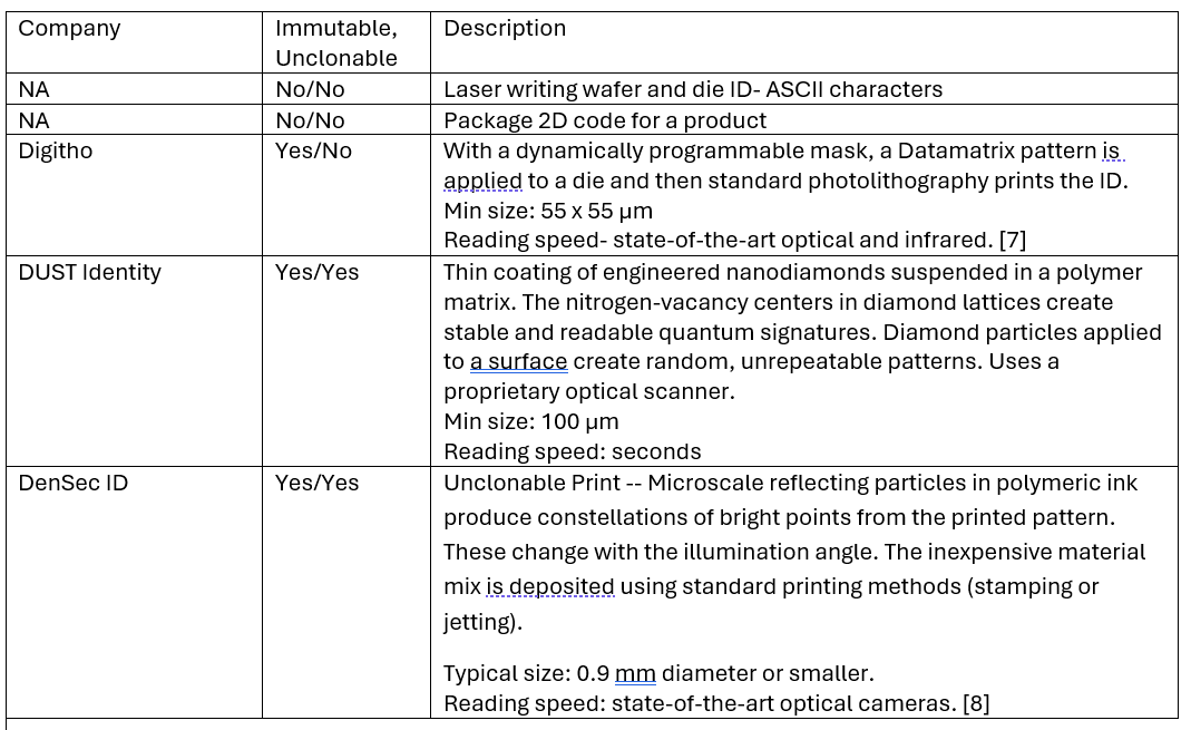
Table 2: Selected extrinsic identifiers.
In the past few years, several start-up companies have developed extrinsic identifiers for chips that are immutable and often unclonable. They vary in technology, speed, and applicability to wafer, substrate or packaged parts.
“The identifier is applied during a photolithography processing step, typically during the patterning of pads or passivation opening steps,” said Richard Beaudry, CEO of Digitho. “A standard photomask is used for patterning the functional features. Then, applying a second exposure on the same resist using a dynamic reprogrammable photomask, the unique identifier code is printed in the photoresist at each die. This can be done at any photolithography step using an i-line stepper. Note that two exposure steps are done, but there is only one developing step. This lithography step is normally done at the wafer level prior to singulation. However, such a step could also be done on reconstructed wafers or panels for die identification.”
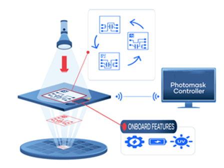
Fig. 2: A dynamically reprogrammable photomask applies a unique data matrix during lithography. Source: Digitho
“To have a link with the package ID, the data matrix can be read at the pick-and-place module, or it can be read during package inspection (visible, IR, or X-ray inspection),” Beaudry said. “The package ID can link to the traceability in the field. In the field reading, it is possible using IR or X-ray inspection. There is a risk that some opaque layers are blocking the reading. De-processing during a failure investigation can retrieve the ID.”
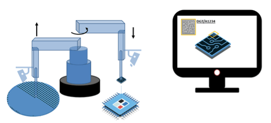
Fig. 3: Illustration showing data matrix being read during the assembly process. Source: Digitho
Assembly components, such as interposers, substrates, and final packages, also need an immutable, unclonable external identifier. Diamond dust applied with a thin film is one such technology. Another technique uses reflective particles within an ink solution.
“With our technology, we can print features anywhere that you can print features and see them with a camera,” said Michael Kozicki, professor of electrical and computer engineering at Arizona State University and CTO at Densec ID Corp. “However, for small parts with small available area, we have been concentrating on jet-deposited dots (UPdots). These could be placed on items as small as surface-mount passive components. We typically use permanent polymers (urethane, polyimide, etc.). We have also been experimenting with removable acrylic so that we could put these patterns on chiplets and have them removed by a hot DI water process prior to assembly.”
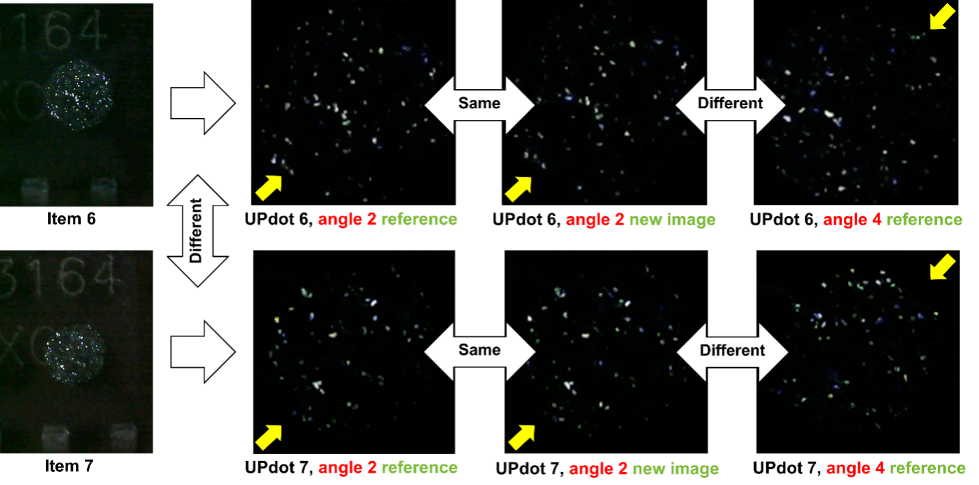
Fig. 4: Constellation examples comparing two prints for the UP print technology, imaged using a digital microscope with illumination at 30° inclination, 315°(1), 225°(2), 135°(3), 45°(4) azimuth. Source: Arizona State University
Mixed-signal, analog, sensors and discretes
With the provenance of a trusted supply chain, integrators have confidence that the ICs and discretes used in their products are reliable. Systems include mixed-signal, analog, and discrete components, which are just as vulnerable to counterfeiting and gray-market activity as digital components [10, 11]. Similarly, smaller logic devices may not be able to implement an intrinsic identifier and thus are also vulnerable.
Critical infrastructure requires many small and inexpensive devices. If the chip industry cannot provide provenance for those devices, then the electronics system cannot be fully trusted. A datacenter rack contains power modules and AI products that depend upon voltage regulators. A military jet depends upon capacitors and resistors that meet military specifications. A public utility depends upon sensors. A cellular tower depends upon RF devices.
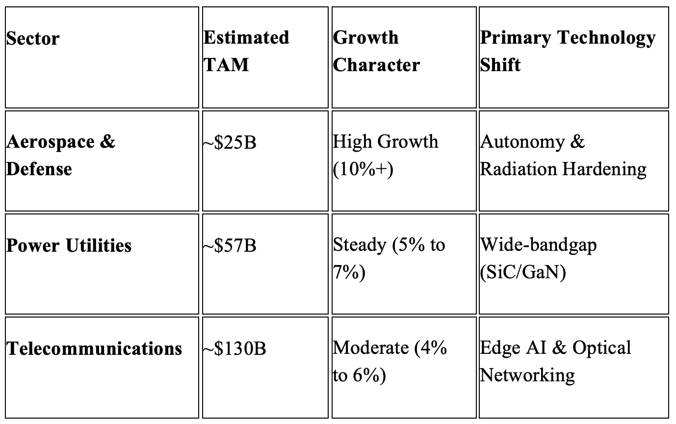
Table 3: 2026 estimate of worldwide total addressable market (TAM) for critical infrastructure semiconductors. Source: Company reports, earnings calls 2025-2026.
Looking at unit volumes provides insights into the scale of traceability and provenance needs as well as the potential vulnerability from untrusted semiconductors. The top five US-based companies dominating critical infrastructure include Intel, Global Foundries, Texas Instruments, Analog Devices, and Microchip.
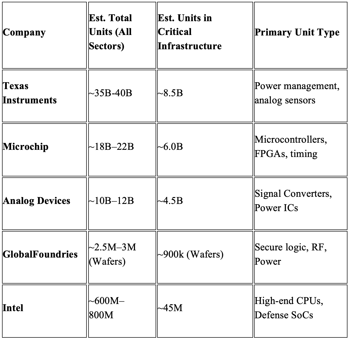
Table 4: Estimated annual unit shipments for 2026 (foundries measured by wafer starts. Source: Public sources for 2025-2026 shipment trends, capacity expansions, and sector-specific demand. Note: Wafers may contain thousands of small devices or dozens of large computing devices.
Governments have begun to mandate ‘trusted silicon’ for these critical infrastructure sectors, and they are willing to pay a premium on chips manufactured in designated regions/countries (e.g., EU, Japan, India, US). That extra cost will help support the needed initial investments to create a trusted supply chain system, as well as the ongoing maintenance for that system.
“Many analog and mixed‑signal devices, such as certain sensor technologies, are not manufactured using CMOS‑based processes, and therefore do not support on‑die memory or integrated identifiers,” said SEMI’s Grupen-Shemansky. “As a result, these devices often lack any built‑in ID, let alone a serialized unique identifier, and tracing them requires a solution to be specifically designed for the device and its manufacturing context. There is no universal approach today, and addressing traceability for such devices may require industry collaboration or consortium‑based efforts to define solutions that align with the realities of the supply chain.”
Others agree. “We have the major underpinnings to implement a trusted supply chain solution,” said Advantest’s Carulli. “It is not a technology issue to enable this, at least for digital chips as a start. There is some innovation needed for smaller devices like AMS-RF ICs, discrete transistors, passive devices, as well as PCB boards.”
Conclusion
End-to-end traceability is a frequently cited need due to the decentralization of electronics production. A trusted supply chain goes one step beyond traceability.
“Adopting a trusted supply chain means embedding identity, authenticity, and accountability into every device and transaction, from wafer to chiplet, PCB, and beyond — and starting from chip design and manufacturing,” said Tom Katsioulas, CEO of Archon Design Solutions. “Identifier technologies anchor trust in silicon. Standards make it interoperable. And policy frameworks make it enforceable. When these converge, trusted supply chain provenance becomes not only a compliance requirement, but a value chain enabler transforming traceability into business advantage.”
Supporting a trusted supply chain out to the end system requires both intrinsic and extrinsic IDs that meet the immutability and non-clonability requirements. While these are widely available for digital components today, they are not available for mixed-signal, analog, sensor ICs as well as passive components and board. Emerging extrinsic IDs could address the technical challenge, but they require further development and eventual adoption. Otherwise, critical infrastructure systems remain vulnerable to counterfeits and gray market ICs, which may endanger lives or disrupt utility services.
References:
- J. Schrijen and V. van der Leest, “Comparative analysis of SRAM memories used as PUF primitives,” 2012 Design, Automation & Test in Europe Conference & Exhibition,
- Rajski, M. Trawka, J. Tyszer and B. Włodarczak, “A Lightweight True Random Number Generator for Root of Trust Applications,” in IEEE Transactions on Computer-Aided Design of Integrated Circuits and Systems, vol. 42, no. 9, pp. 2815-2825, Sept. 2023,
- Rajski, M. Trawka, J. Tyszer and B. Włodarczak, “H2B: Crypto Hash Functions Based on Hybrid Ring Generators,” in IEEE Transactions on Computer-Aided Design of Integrated Circuits and Systems, vol. 43, no. 2, pp. 442-455, Feb. 2024,
- J. Parker et al., “A Physical Unclonable Function Leveraging Hot Carrier Injection Aging,” 2023 IEEE International Reliability Physics Symposium,
- Jeon, J. H. Baek, D. K. Kim and B. -D. Choi, “Towards Zero Bit-Error-Rate Physical Unclonable Function: Mismatch-Based vs. Physical-Based Approaches in Standard CMOS Technology,” 2015 Euromicro Conference on Digital System Design,
- https://www.pufsecurity.com/document/puf-series-3-the-quantum-tunneling-mechanism-of-neopuf/
- https://digitho.com/solutions/programmable-photomask/ and
- N. Kozicki, Authentication Of Identifiers By Light Scattering, US Patent 12307323-B , May 20, 2025.
- https://en.wikipedia.org/wiki/Data_Matrix
- “AFRL concerned about alleged ‘counterfeit’ ejection seat parts, federal lawsuit contends, P Thomas Gnau, Dayton Daily News, September 15, 2022. Link
- “Deceased Pilot’s Widow Sues USAF Over Faulty Ejection Seat,”4, AERO News Network, September 16 2022. Link
Related Articles
Fingerprinting Chips For Traceability
Diverse identifier technologies enable fingerprinting for all device types.
Plugging Gaps In The IC Supply Chain
Consistent unique identifiers, from die to final end-system, open the door for new analytic workflows that can improve reliability and traceability.
Infusing Trust Into The Supply Chain
Why another layer of tracking is needed to transform traceability into trustability.
New Rules Put The Squeeze On Semiconductor Gray Market
Customer demand for trusted components is forcing new investments and cooperation.
Where Cryptography Is Headed
Security teams are scrambling to devise technology that keeps data secure in an era of virtually unlimited compute power.


